
 &n𒅌bsp;
Hello,Please login
&n𒅌bsp;
Hello,Please login
HT7166
13V,10A Fully-Integrated Synchronous Boost Converter
The HT7166 is a high-power density, fully integrated synchronous boost converter with a 16mΩ power switch and a 23mΩ rectifier switch to provide a high efficiency and small size solution in portable systems. The HT7166 has wide input voltage range from 2.7 V to 13 V to support applications with single cell and two cell Lithium batteries. The device has 10A switch current capability and can provide an output voltage up to 13V.The HT7166 uses adaptive constant off-time peak current control topology to regulate the output voltage. In moderate to heavy load condition, it works in the PWM mode. In light load condition, the device works in the PFM mode to improve the efficiency. The switching frequency in the PWM mode is fixed.The HT7166 also implements a fix soft-start function and a fixed switching peak current limit function. In addition, the device provides 14V output overvoltage protection, cycle-by-cycle overcurrent protection, and thermal shutdown protection
米乐m6:DOWNLOAD THE DATA
FEATURES
| APPLICATIONS
|

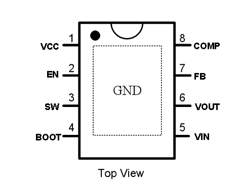
TERMINAL FUNCTION
| TerminalNo. | NAME | I/O* | Description |
| 1 | VCC | O | Output of the internal regulator. A ceramic capacitor of 2.2uF is required between this pin and ground. |
| 2 | EN | I | Enable logic input. Logic high level enables the device. Logic low level disables the device and turns it into shutdown mode. |
| 3 | SW | PWR | The switching node pin of the converter. |
| 4 | BOOT | O | Power supply for high-side MOSTFET gate driver. A ceramic capacitor of 0.1μF must be connected between this pin and the SW pin. |
| 5 | VIN | I | IC power supply input. |
| 6 | VOUT | PWR | Boost converter output. |
| 7 | FB | I | Voltage feedback. |
| 8 | COMP | O | Output of the internal error amplifier, the loop compensation network should be connected between this pin and the GND pin. |
| 0 | GND | PWR | Power ground of the IC. |